
 mattandClaude
ad9c457ea7
Implements ESP32_Soil_Moisture_Node_PRD.md on the VCC-GND Studio
YD-ESP32-S3 (ESP32-S3-WROOM-1) using Arduino via PlatformIO, publishing
to Home Assistant over MQTT with auto-discovery.

Two power profiles behind a compile-time switch (PRD 4):
  -e mains    always on, publishes every 60s
  -e battery  RTC wake, sample, publish, deep sleep 15min

PRD mitigations:
  - All six probes on ADC1 (GPIO4-9); ADC2 is unusable while Wi-Fi is up.
  - analogReadMilliVolts() for eFuse ADC calibration rather than raw counts.
  - 16 samples per probe, sorted, 10% trimmed from each end, averaged.
  - Per-probe two-point calibration; HW-390 output is inverted (dry reads
    high), and an inverted config is rejected rather than silently producing
    a backwards curve.
  - MAC-derived node ID so identical binaries never collide on topics.

Design decisions that diverge from a literal reading of the PRD:
  - Out-of-range probes publish null (HA "unknown") instead of clamping to
    0%/100%. A cut Cat5 pair reads ~0mV, which clamps to a believable "very
    dry" and would drive irrigation on wrong data.
  - The battery profile uses expire_after rather than an availability topic;
    a sleeping node is offline most of the time and would sit greyed out.
  - AWAKE_BUDGET_MS forces deep sleep if a wake cycle overruns, covering
    failure modes the per-step network timeouts miss (DHCP never issued,
    CONNACK never sent) that would otherwise flatten the cell.
  - docs/WIRING.md notes the 18650 cannot feed the probes directly: the
    XC6206 LDO needs ~3.4V headroom, so a boost converter is required on the
    switched side of the MOSFET.

Both profiles compile clean under -Wall. Not yet run on hardware; pin map,
MOSFET circuit and calibration defaults are unverified against a board.

Co-Authored-By: Claude <noreply@anthropic.com>
114 lines
5.9 KiB
XML
114 lines
5.9 KiB
XML
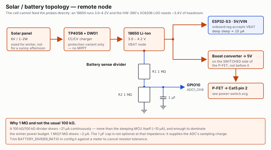


<svg xmlns="http://www.w3.org/2000/svg" xmlns:xlink="http://www.w3.org/1999/xlink" viewBox="0 0 940 520" width="940" height="520" role="img" aria-labelledby="t4">
|
||
<title id="t4">Solar and battery power topology with boost converter and battery sense divider</title>
|
||
<style>
|
||
.bg { fill: #fcfcfa; }
|
||
.ttl { font: 600 19px ui-sans-serif, system-ui, 'Segoe UI', Roboto, sans-serif; fill: #16181d; }
|
||
.h { font: 600 13px ui-sans-serif, system-ui, 'Segoe UI', Roboto, sans-serif; fill: #16181d; }
|
||
.s { font: 11.5px ui-sans-serif, system-ui, 'Segoe UI', Roboto, sans-serif; fill: #6b7280; }
|
||
.m { font: 11px ui-monospace, SFMono-Regular, Menlo, Consolas, monospace; fill: #374151; }
|
||
.box { fill: #f3f4f6; stroke: #16181d; stroke-width: 1.6; }
|
||
.boxp { fill: #fff3ec; stroke: #c2410c; stroke-width: 1.8; }
|
||
.boxs { fill: #eef2ff; stroke: #1d4ed8; stroke-width: 1.8; }
|
||
.pw { fill: none; stroke: #c2410c; stroke-width: 2.2; }
|
||
.sigw { fill: none; stroke: #1d4ed8; stroke-width: 1.8; }
|
||
.gw { fill: none; stroke: #374151; stroke-width: 1.9; }
|
||
.comp { fill: #ffffff; stroke: #16181d; stroke-width: 1.5; }
|
||
</style>
|
||
|
||
<rect class="bg" x="0" y="0" width="940" height="520"/>
|
||
<text class="ttl" x="20" y="30">Solar / battery topology — remote node</text>
|
||
<text class="s" x="20" y="49">The cell cannot feed the probes directly: an 18650 runs 3.0–4.2V and the HW-390's XC6206 LDO needs ~3.4V of headroom.</text>
|
||
|
||
<!-- ============ chain ============ -->
|
||
<rect class="boxp" x="24" y="96" width="150" height="80" rx="6"/>
|
||
<text class="h" x="38" y="120">Solar panel</text>
|
||
<text class="m" x="38" y="139">6V / 1–2W</text>
|
||
<text class="s" x="38" y="158">sized for winter, not</text>
|
||
<text class="s" x="38" y="171">for a sunny afternoon</text>
|
||
|
||
<path class="pw" d="M174,136 L216,136" marker-end="url(#ar)"/>
|
||
|
||
<rect class="boxp" x="222" y="96" width="160" height="80" rx="6"/>
|
||
<text class="h" x="236" y="120">TP4056 + DW01</text>
|
||
<text class="m" x="236" y="139">CC/CV charger</text>
|
||
<text class="s" x="236" y="158">protection variant only</text>
|
||
<text class="s" x="236" y="171">— no MPPT</text>
|
||
|
||
<path class="pw" d="M382,136 L424,136" marker-end="url(#ar)"/>
|
||
|
||
<rect class="boxp" x="430" y="96" width="140" height="80" rx="6"/>
|
||
<text class="h" x="444" y="120">18650 Li-Ion</text>
|
||
<text class="m" x="444" y="139">3.0 – 4.2 V</text>
|
||
<text class="s" x="444" y="158">VBAT node</text>
|
||
|
||
<!-- split to MCU and boost -->
|
||
<circle cx="600" cy="136" r="4" fill="#c2410c"/>
|
||
<path class="pw" d="M570,136 L600,136"/>
|
||
<path class="pw" d="M600,136 L600,86 L716,86" marker-end="url(#ar)"/>
|
||
<path class="pw" d="M600,136 L600,206 L716,206" marker-end="url(#ar)"/>
|
||
|
||
<rect class="boxs" x="722" y="56" width="192" height="62" rx="6"/>
|
||
<text class="h" x="736" y="79">ESP32-S3 · 5V/VIN</text>
|
||
<text class="s" x="736" y="97">onboard reg accepts VBAT</text>
|
||
<text class="m" x="736" y="112">deep sleep ≈ 10 µA</text>
|
||
|
||
<rect class="boxp" x="722" y="176" width="192" height="62" rx="6"/>
|
||
<text class="h" x="736" y="199">Boost converter → 5V</text>
|
||
<text class="s" x="736" y="217">on the SWITCHED side of</text>
|
||
<text class="s" x="736" y="231">the P-FET, not before it</text>
|
||
|
||
<path class="pw" d="M818,238 L818,282" marker-end="url(#ar)"/>
|
||
<rect class="boxp" x="722" y="288" width="192" height="54" rx="6"/>
|
||
<text class="h" x="736" y="310">P-FET → Cat5 pin 2</text>
|
||
<text class="s" x="736" y="329">see power-switch.svg</text>
|
||
|
||
<!-- ============ battery sense divider ============ -->
|
||
<path class="sigw" d="M500,176 L500,222"/>
|
||
<circle cx="500" cy="176" r="4" fill="#c2410c"/>
|
||
<text class="h" x="300" y="228">Battery sense divider</text>
|
||
|
||
<rect class="comp" x="480" y="222" width="40" height="52" rx="2"/>
|
||
<text class="m" x="528" y="252">R1 1 MΩ</text>
|
||
|
||
<path class="sigw" d="M500,274 L500,302"/>
|
||
<circle cx="500" cy="302" r="4" fill="#1d4ed8"/>
|
||
<path class="sigw" d="M500,302 L640,302" marker-end="url(#ab)"/>
|
||
<text class="h" x="648" y="299">GPIO10</text>
|
||
<text class="s" x="648" y="315">ADC1_CH9</text>
|
||
|
||
<!-- shunt cap -->
|
||
<path class="sigw" d="M566,302 L566,336"/>
|
||
<circle cx="566" cy="302" r="3.4" fill="#1d4ed8"/>
|
||
<line x1="555" y1="336" x2="577" y2="336" stroke="#16181d" stroke-width="1.8"/>
|
||
<line x1="555" y1="342" x2="577" y2="342" stroke="#16181d" stroke-width="1.8"/>
|
||
<path class="gw" d="M566,342 L566,368"/>
|
||
<use xlink:href="#gnd" href="#gnd" x="566" y="368"/>
|
||
<text class="m" x="584" y="342">1 µF</text>
|
||
|
||
<rect class="comp" x="480" y="302" width="40" height="52" rx="2"/>
|
||
<text class="m" x="410" y="332">R2 1 MΩ</text>
|
||
<path class="gw" d="M500,354 L500,382"/>
|
||
<use xlink:href="#gnd" href="#gnd" x="500" y="382"/>
|
||
|
||
<!-- ============ notes ============ -->
|
||
<rect x="20" y="410" width="900" height="90" rx="5" fill="#fff3ec" stroke="#c2410c" stroke-width="1.4"/>
|
||
<text class="h" x="34" y="431">Why 1 MΩ and not the usual 100 kΩ.</text>
|
||
<text class="s" x="34" y="450">A 100 kΩ/100 kΩ divider draws ~21 µA continuously — more than the sleeping MCU itself (~10 µA), and enough to dominate</text>
|
||
<text class="s" x="34" y="468">the winter power budget. 1 MΩ/1 MΩ draws ~2 µA. The 1 µF cap is not optional at that impedance: it supplies the ADC's sampling charge.</text>
|
||
<text class="s" x="34" y="486">Trim BATTERY_DIVIDER_RATIO in config.h against a meter to cancel resistor tolerance.</text>
|
||
|
||
<defs>
|
||
<marker id="ar" markerWidth="9" markerHeight="9" refX="8" refY="4.5" orient="auto">
|
||
<path d="M0,0 L9,4.5 L0,9 z" fill="#c2410c"/>
|
||
</marker>
|
||
<marker id="ab" markerWidth="9" markerHeight="9" refX="8" refY="4.5" orient="auto">
|
||
<path d="M0,0 L9,4.5 L0,9 z" fill="#1d4ed8"/>
|
||
</marker>
|
||
<g id="gnd">
|
||
<line x1="-10" y1="0" x2="10" y2="0" stroke="#374151" stroke-width="1.9"/>
|
||
<line x1="-6" y1="4.5" x2="6" y2="4.5" stroke="#374151" stroke-width="1.9"/>
|
||
<line x1="-2.5" y1="9" x2="2.5" y2="9" stroke="#374151" stroke-width="1.9"/>
|
||
</g>
|
||
</defs>
|
||
</svg>
|